Building the Frog Sounds QRP Kit 3: Key Circuitry
When the power supply was done it felt reasonable to continue with the key circuitry, because the key is an input to most of the other blocks. This post describes the key jack with pull up network, the LED indicator circuit, and the NAND gates that function as a buffer and beeper. The reference designators in the schematics here match those in the schematic that was included in the kit.
LED Indicator Circuit
The external key is connected to J3. When the key is pressed, the
KEY node in the circuit is shorted to ground potential. When the key
is up, the KEY node is pulled up by R13 and D2 to about 4
volts. The KEY node is connected the LED indicator circuit, the
mixer, and the audio amplifier.
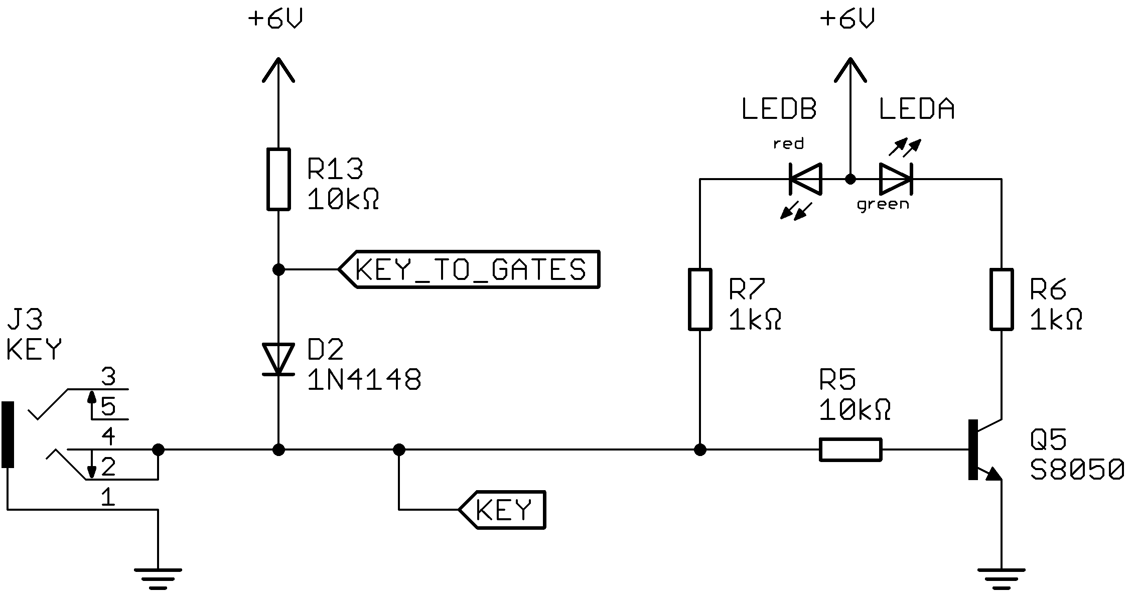
Figure 1. Schematic of the key pull up network and the indicator circuit
The bi-color LED lights up in green when the key is up indicating
reception, and red when the key is down indicating transmission. When
the key is pressed, current flows through LEDB (red), R7, and the
key. Because the KEY node is at 0 volts, no current flows through
the base of Q5, turning it off and cutting off LEDA (green).
When the key is up, current flows through R13, D2, R5, and the
base of Q5, turning it on. Current can then flow through LEDA
(green), R6, and the Q5 collector. It sounds reasonable for the
red LEDB to be off in this scenario. To my surprise when I built the
circuit it still shone quite noticeably when the key was up. This
brings me to the build experience.
Building and Troubleshooting
Soldering the indicator circuit went smooth, but as soon as I turned on the power I noticed that the red part of the bi-color LED never quite turned off, resulting in a yellow color (Figure 2). I first suspected that I had damaged some component, so I went on and measured all the voltages, both with the key up and down, but they all seemed reasonable.

Figure 2. Red LED not turning off
I started to think about where the current though the red LED could
possibly go, and by the process of elimination I realized that it must
go through R5 and the base of Q5. I had dismissed the base current
because it is usually a small control current, but in this case it was
actually driving the red LED! The current snaked through LEDA (red),
R7, R5, and finally the base and emitter of Q5.
If figured out that if I increased the value of R5 the current would decrease and eventually the red LED would go dark. A too high value of R5 would keep Q5 from being sufficiently turned on when the key was down, though. It was time to experiment to see which values worked.
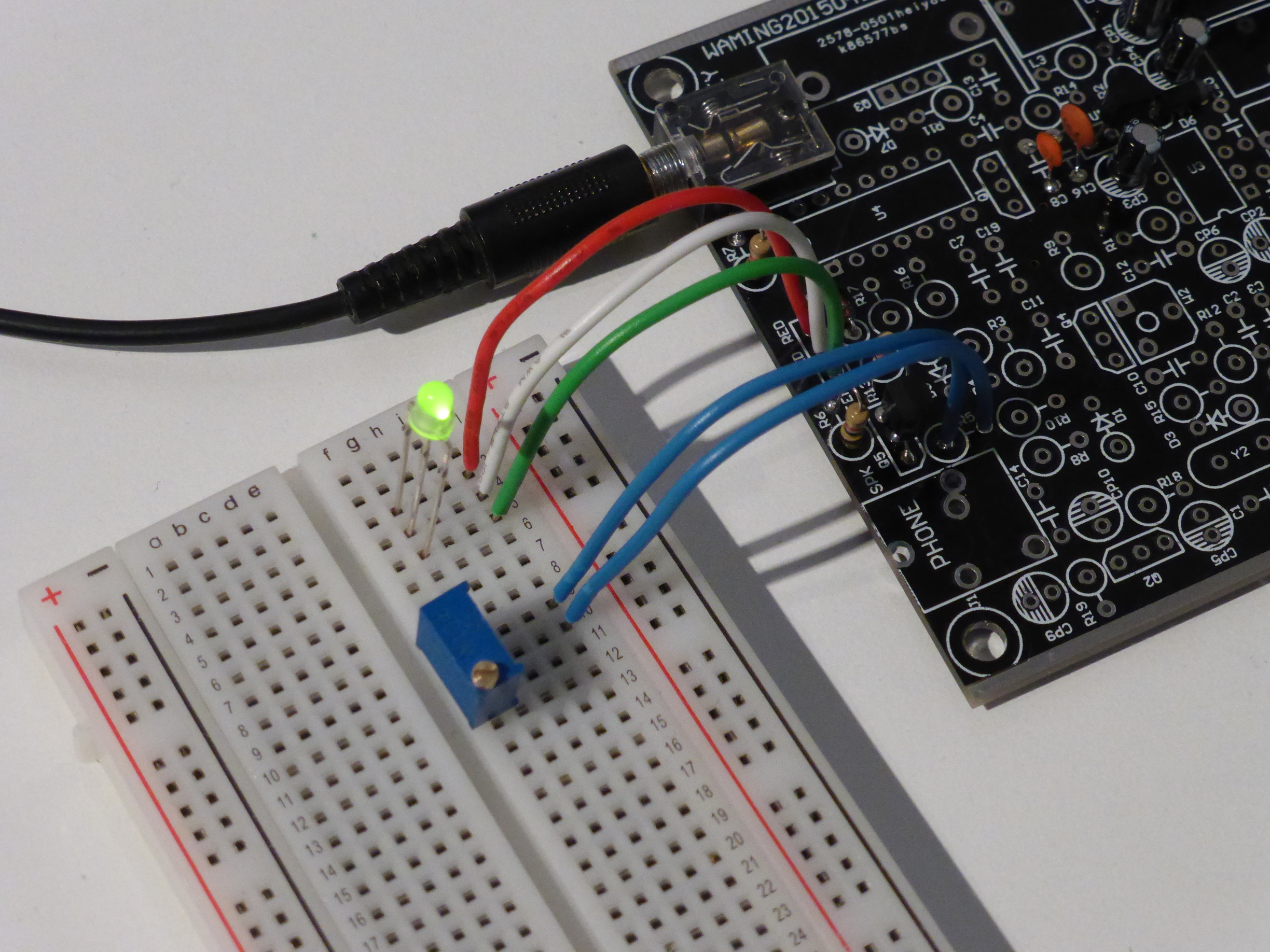
Figure 3. R5 tuning experiment
I desoldered the 10 kΩ R5 resistor and replaced it temporarily with a 100 kΩ potentiometer (Figure 3). I found that any value over 35 kΩ was enough to turn off the red LED. The green green LED was on for the whole range of the potentiometer. Therefore, I could safely pick any value between 35 and 100 kΩ, and I settled somewhat arbitrarily on a 47 kΩ resistor since I had one around. I soldered the new 47 kΩ R5 in place and the indicator worked great!
NAND Gate Buffer and Beeper
The U4 74HC00 quad NAND gate IC is used for two purposes. The first
is to buffer the KEY signal to logic levels. The second is to
generate a beep on the audio output jack when the key is pressed.
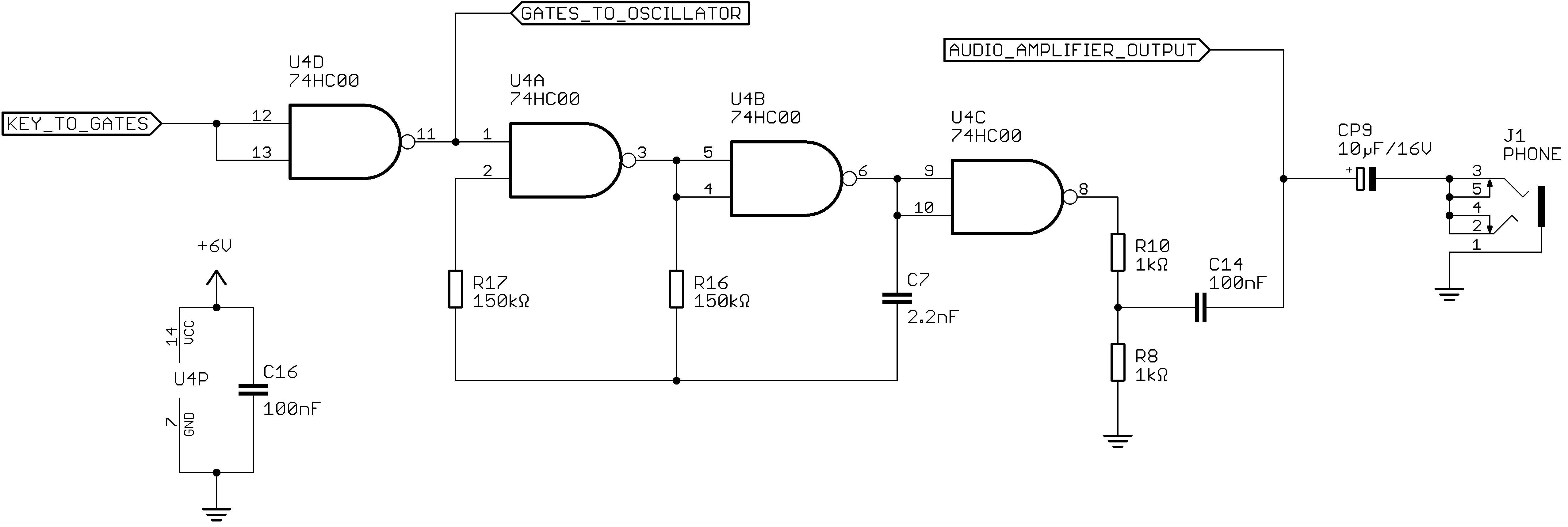
Figure 4. Schematic of the NAND gates block
The node between R13 and D2 is used as the input to the NAND
gates. Its potential remains one diode voltage drop above the KEY
node and is about 4.5 volts on key up and 0.6 volts on key down. These
values are within range for the U4D inputs.
The U4D gate buffers and inverts the key signal. Its output is fed
to the U4A input, and later also to the RF oscillator block. The
U4A, U4B, and U4C gates, along the R17, R16, and C7
passives, form a "beeper" oscillator. During the time the key is
pressed, the oscillator generates a square wave at about 800 Hz.
While building this part I found out that C7 was 4.7 nF in the
schematic but 2.2 nF in the component list. I used a 2.2 nF capacitor
since it was the one actually included in the kit, and updated my
schematic accordingly.
The square wave is then attenuated by the R10-R8 voltage divider
and connected through the C14 and CP9 coupling capacitors to the
J1 audio output jack. The output of the audio amplifier block is
also connected between the coupling capacitors. The idea seems to be
that only one of the two audio sources (the audio amplifier and the
beeper oscillator) is active at any point in time. On key down the
audio amplifier output is actually disconnected by a transistor (more
about that in a later post). On key up, the beeper U4C gate remains
connected but is constantly high, so the R10-R8 voltage divider
ought to load the audio amplifier output somewhat, I think.
While testing the beeper I found that the beeper frequency was
noticeably unstable. If I touched the C7 capacitor, it gradually
rose to at least 900 Hz. When not touching the capacitor it slowly
dropped towards 800 Hz again.
Conclusion
With the beeper circuit done, the kit starts to become useful. With the extruded aluminum enclosure in place, the kit almost looks finished! Because there are no radio related parts in it yet, it only works as a Morse code practice device. Even then, I had some fun with it, as can be seen in the video below.
Next time I will either continue with the RF oscillator/mixer or the audio amplifier. If you find any inaccuracies in this post, or have any question please write a line in the comments below. Stay tuned!
DE RAEK 73
Comments
Comments are hosted on the same server as this blog. The server resides in the EU and no data is shared with third parties.