Building the Frog Sounds QRP Kit 2: Power Supply
The first block I started to solder was the power supply. Figure 1 show its schematic.
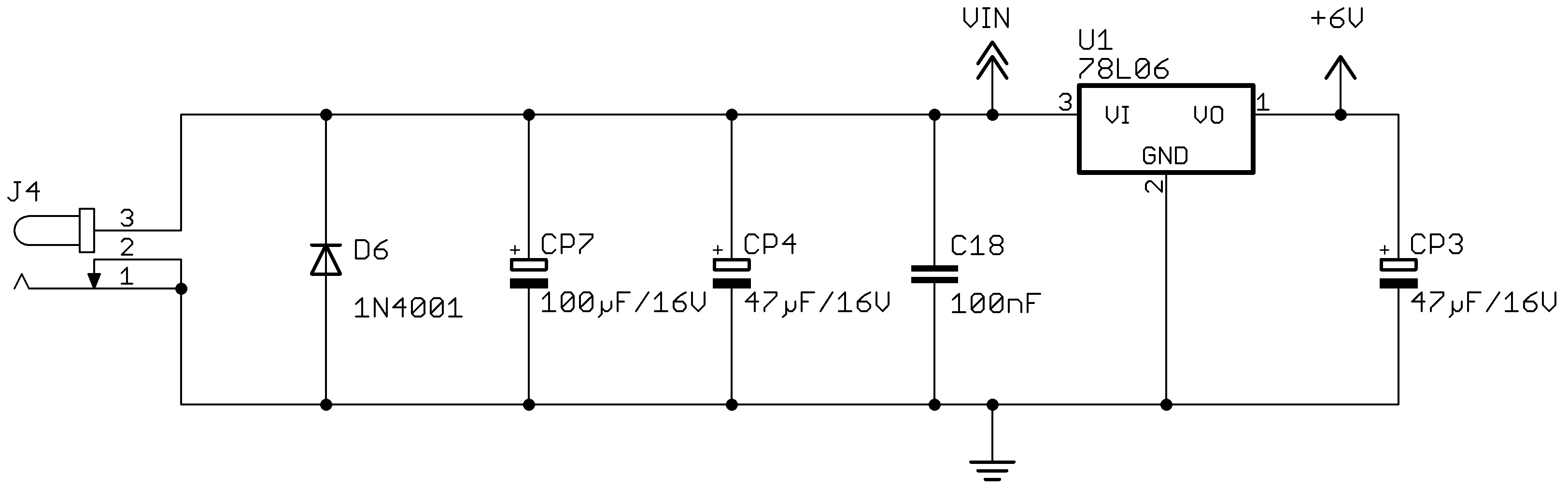
Figure 1. Schematic of the power supply block
EDIT 2015-10-17: Renamed diode to D6 to match schematic included
in kit. Corrected C18 value to 100 nF.
Block Description
The board has two power domains. The external voltage of 9 to 12 volts is used by the power hungry blocks, namely the RF amplifier and the audio amplifier. An internally regulated voltage of 6 volts is used by the mixer/oscillator, the logic gates and the bi-color LED because they need a fixed voltage.
The central component of the power supply is the 78L06 linear power regulator. Capacitors are placed at the regulator input and the output as expected. The 1N4001 diode protects the board from accidentally connecting the external power in reverse. If it has the wrong polarity the diode causes a short circuit, which hopefully blows a fuse in the external power supply and spares the rest of the board.
Build and Test
The power supply was the first block I soldered. The result can be seen in Figure 2. When I soldered it I discovered two issues with the design. They might be rather harmless, but I thought they would be interesting to point out.
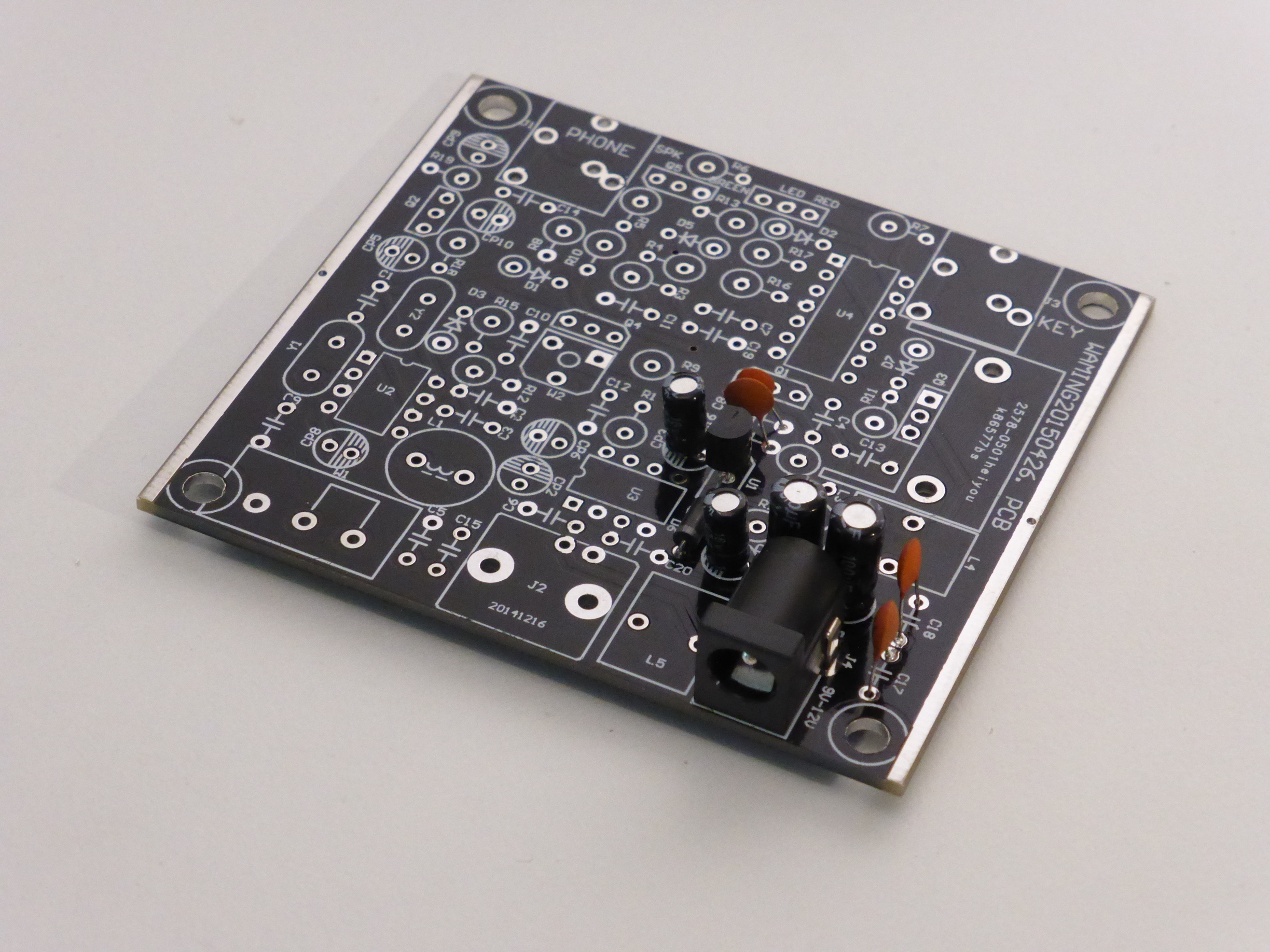
Figure 2. The power supply block soldered
The first issue is that the printed circuit board does not have thermal relief pads. In other words, a pad connected to ground is just a hole through the ground plane. The ground plane conducts heat well, so the soldering iron needs to be hotter or held at place longer. In a thermal relief pad, the pad and the ground plane are separated by a small ring shaped gap that is bridged with a few thin traces. Thermal relief pads are easier to solder, but they might have disadvantages I don't know about.
The other issue was that the decoupling capacitors were all placed together in a cluster near the power supply. I decided to solder them too in order to finish the power supply area of the board. As can be seen in Figure 3, the trace from component to decoupling capacitor is a bit long for C17-L3 (red), C8-U2 (green), and C16-U4 (blue).
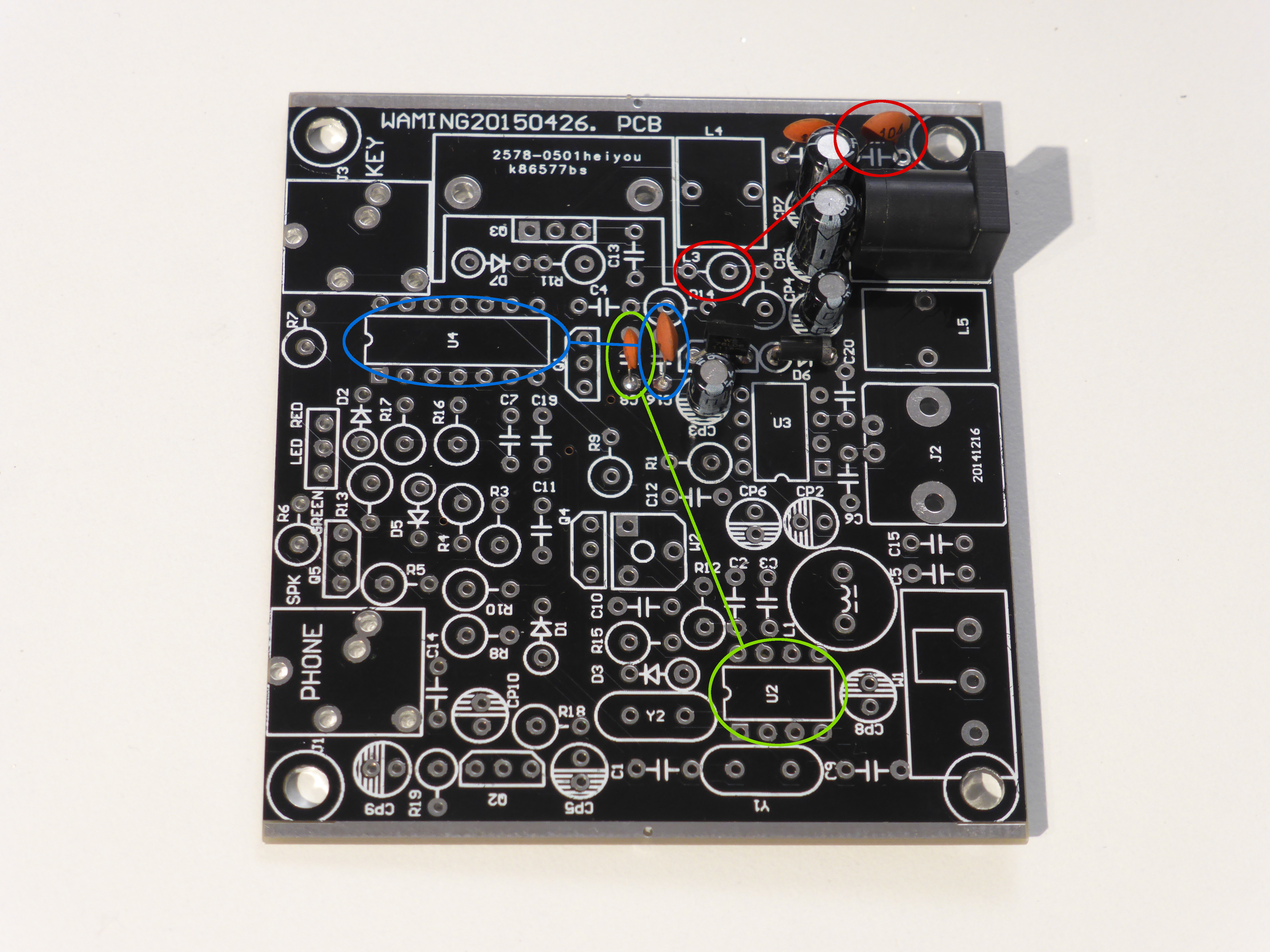
Figure 3. Decoupling capacitors and components they relate to
A power supply will not be able to keep the voltage constant when the current is sufficiently high and the rate of change of the current is sufficiently fast. Decoupling capacitors are used near current drawing components to compensate for that the power supply that cannot regulate the voltage quickly enough. A long wire between the current consuming component and the decoupling capacitor can be a problem since it will act as an antenna and emit electromagnetic radiation, which can then enter other components and cause interference.
I will put the board in an aluminum enclosure which will shield the board and the outside world from each other. So in my case the long wires will probably not be a problem unless the transceiver happens to interfere heavily with itself.
Testing the power supply was not very exciting. I checked that the protection diode conducted in the correct direction using the diode test mode of my multimeter. When I powered up the board the on-board regulator produced 5.9 volts, which is well in the range of what the ICs need.
That's it for now. If you find any inaccuracies in this post, please let me know in a comment below. Next post will also feature a seemingly mundane block: the bi-color LED indicator. It did not behave correctly so I analyzed the circuit and did some modifications. Stay tuned!
DE RAEK 73
Comments
Comments are hosted on the same server as this blog. The server resides in the EU and no data is shared with third parties.